Internship @ Hewlett Packard Enterprise
10 MHz & 1PPS Reference Switching Circuit
Selected and qualified a replacement analog switch for a 10 MHz / 1PPS reference distribution circuit, then owned the redesign from schematic through bring-up and G.703 validation.
Work from my hardware internship on the networking R&D team, described at a general signal-integrity level, with no proprietary designs or details.
Context
The 10 MHz frequency reference and the 1PPS (one-pulse-per-second) timing edge are the backbone that downstream logic locks onto. A reference-distribution circuit selects between reference sources and fans those signals out cleanly, so anything it adds, whether noise, jitter, or leakage, propagates into everything that depends on the reference. That puts a high bar on the distribution path.
The switch at the center of that path carries an off-isolation requirement: when a channel is switched off, whatever sits on that input has to be strongly attenuated so it can’t bleed into the output. This board was failing that requirement. Reference signals were leaking through in the switch’s off state, above the allowed level.
Root-causing the failure
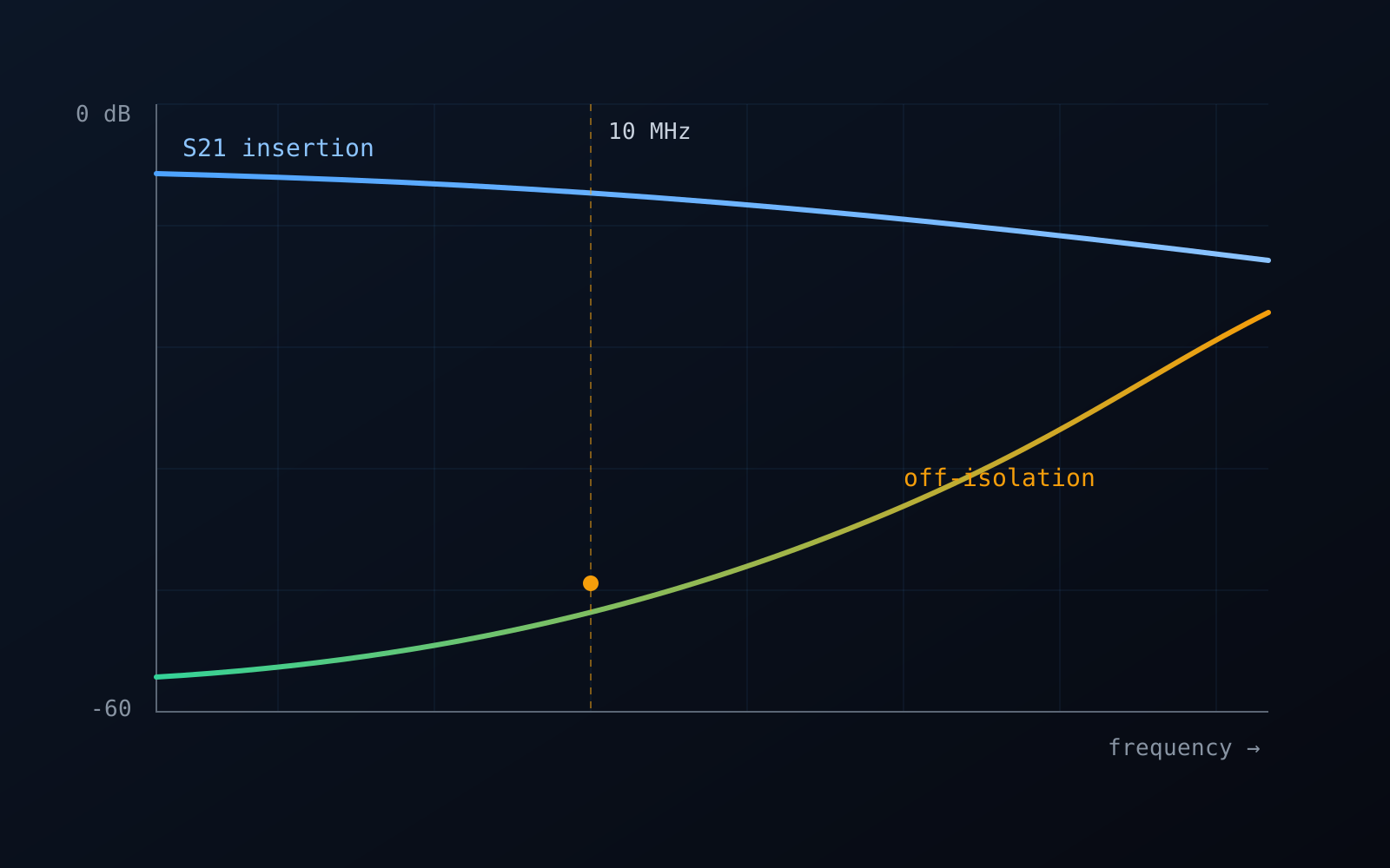
Instead of swapping parts and hoping, I measured channel attenuation stage by stage, across the analog switch, the current buffer, and the comparator, to localize where the leakage was actually originating. That isolated the fault to the analog switch itself: 23 dB of off-isolation at 10 MHz against a 40 dB datasheet specification.
The mechanism is the switch’s off-state feedthrough. Even when it’s “open,” a switch presents a small feedthrough capacitance that forms a high-pass leakage path, so off-isolation degrades as frequency rises. By 10 MHz, that parasitic coupling, together with crosstalk in the off state, was enough to push the channel past spec.
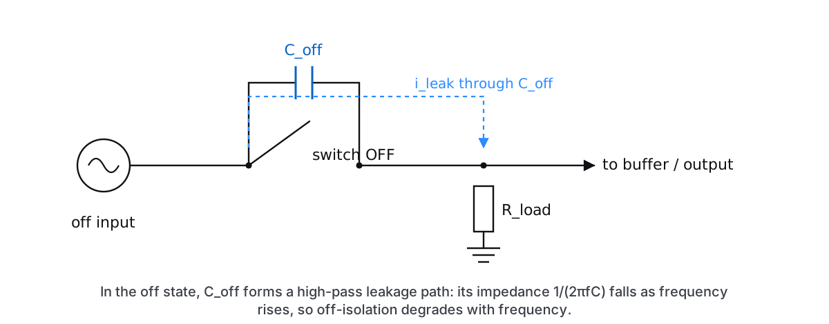
Off-state model: even “open,” the switch presents a small feedthrough capacitance that bridges input to output. Its impedance falls as frequency rises, which is why off-isolation degrades.
Qualifying a replacement
I characterized candidate switches on a vector network analyzer, turning each part’s behavior into S-parameters I could compare directly, and scored them on the parameters that actually decide this trade-off:
- Off-isolation: how hard the off channel is attenuated (the spec that was failing).
- Feedthrough capacitance (C_off): the root cause of isolation roll-off with frequency.
- On-resistance (R_on): sets insertion loss and on-state signal integrity.
- Bandwidth: has to comfortably cover the reference frequencies.
These pull against one another, since a part with very low C_off can cost bandwidth or on-resistance, so the selection was about clearing the off-isolation requirement with margin while keeping the on-state performance the reference path needs.
Owning the redesign through bring-up
I carried the fix from schematic and isolation-conscious layout through fabrication and bring-up. The layout goal was to keep off-state coupling low: routing the aggressor and victim nets with that in mind, minimizing the parasitics around the switch, and using grounding to keep stray coupling off the output.
Validation
I validated the reworked path’s insertion loss and return loss against ITU-T G.703, the ITU standard defining the electrical characteristics for this class of timing/reference interface, to confirm the redesign met the requirement it had been failing.