Personal
BMS Cell Simulator
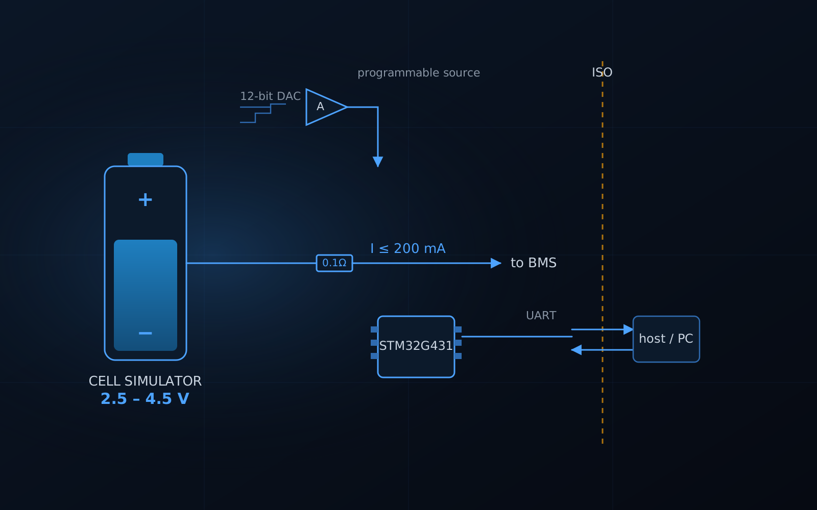
An isolated single-cell battery emulator for bench-testing Battery Management Systems: a programmable 2.5–4.5 V / 200 mA source with on-board current sensing, driven by an STM32G431 over serial and designed to stack in series to emulate a full pack.
Overview
A circuit that simulates a single battery cell so a Battery Management System (BMS) can be tested on the bench without a real pack. The simulator presents a programmable voltage from 2.5 V to 4.5 V, sources up to 200 mA, and measures the current the BMS draws while balancing. An STM32G431CBT6 sets the voltage and reports the measured current to a computer over serial. The whole simulator runs in an isolated power domain so that multiple units can be stacked in series to emulate a full pack. I designed the schematic and PCB layout in KiCad.
Voltage generation
Target: an adjustable 2.5–4.5 V output that holds within 5% while sourcing up to 200 mA.
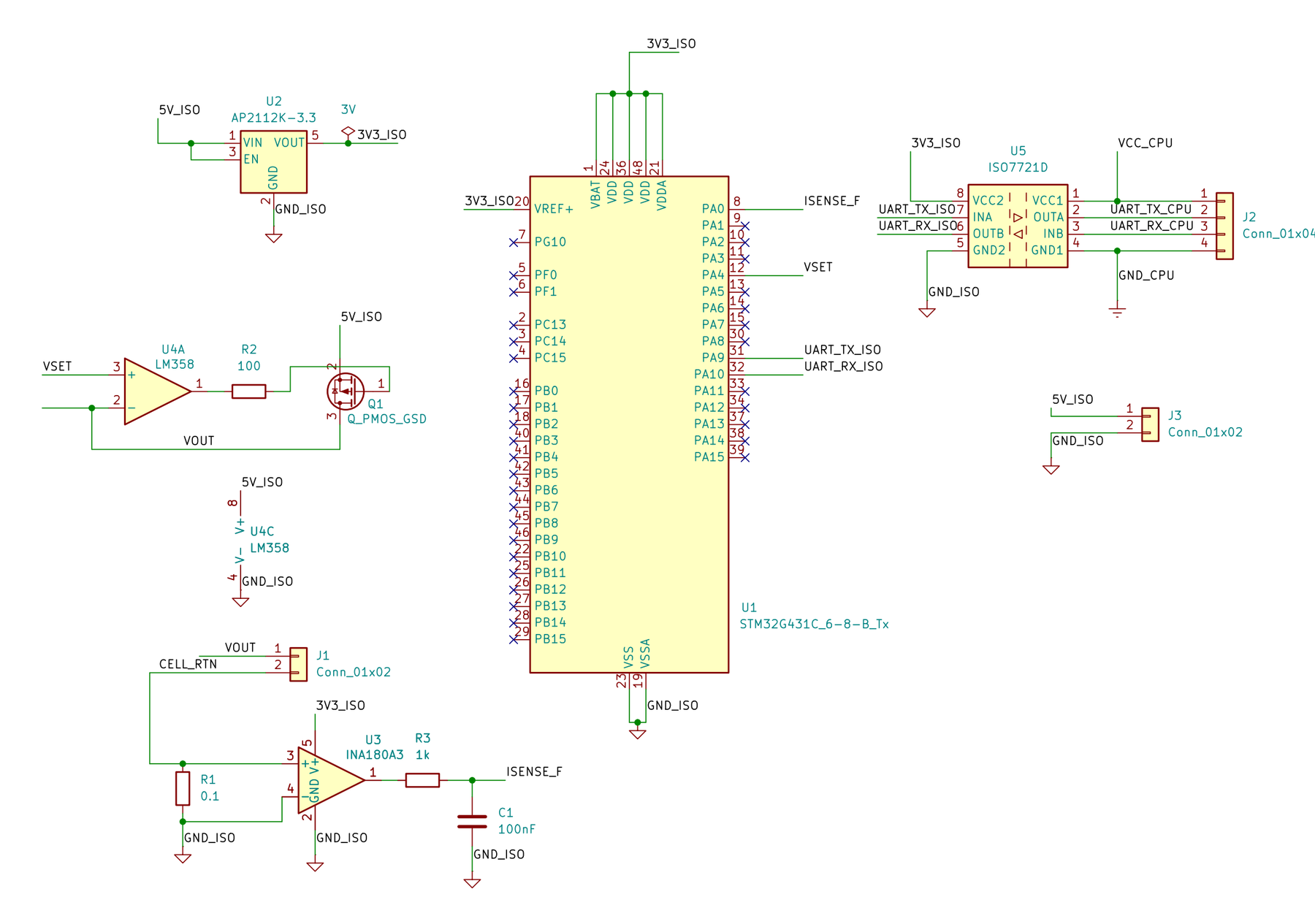
- I used the STM32’s internal 12-bit DAC to set the target, followed by an op-amp and a P-channel MOSFET pass device in a closed feedback loop. The op-amp compares the DAC setpoint against the actual output and drives the gate until they match, holding the output regardless of load.
- Internal DAC over an external part. 12 bits gives sub-millivolt steps, ~two orders of magnitude finer than the 5% spec, so it saves a component with no accuracy penalty.
- Linear over switching regulation. Worst-case dissipation in the pass device is only ~0.5 W. At that level a switcher’s efficiency edge is irrelevant and would only add noise and EMI to a circuit whose whole job is a clean, precise voltage.
- P-channel high-side over an N-channel follower. An LM358 on the 5 V rail can’t swing high enough to turn on an N-channel follower for a 4.5 V output. A P-channel device turns on when its gate is pulled toward ground, which the op-amp does easily, so it reaches full range on a single 5 V rail.
Current measurement
Target: measure output current up to 200 mA within 10% and report it.
- Low-side shunt → fixed-gain current-sense amp (INA180A3, gain 100) → RC filter → internal ADC. A 0.1 Ω shunt drops 20 mV at 200 mA (just 4 mW dissipation); a gain of 100 scales that to 2 V, filling most of the 3.3 V ADC range for good resolution while staying safely below the rail.
- Dedicated current-sense amp over a discrete op-amp. Its gain is set by internal precision-matched resistors, improving accuracy and reducing part count.
- Low-side over high-side sensing. The signal sits near ground where it’s easy to amplify, and it keeps the shunt out of the output path so it doesn’t eat into the pass stage’s headroom. With a loose 10% tolerance, a simple RC filter plus firmware averaging meets spec comfortably.
Communication & isolation
- UART from the STM32 across an ISO7721 digital isolator, with an off-the-shelf USB-to-serial cable handling the USB conversion on the computer side.
- I rejected native USB from the STM32 because it would tie the computer’s ground into the isolated domain and defeat the isolation. Routing UART through a digital isolator keeps the barrier intact while still presenting a standard serial port.
- I pushed the USB-to-serial conversion off the board into a standard cable. Since this is bench test equipment, not a shipped product, that cuts board complexity for the same function.
- Isolation was the constraint underneath everything: an isolated 5 V supply means the simulator is
meant to float, so the whole design stays in one floating domain referenced to
GND_ISO, crossing the barrier only through the isolator (independent power and ground on each side). That’s what lets units stack in series to emulate a full pack.
Firmware
- An interrupt-driven main loop rather than an RTOS (the task set is small and doesn’t justify the overhead), organized in three layers: a HAL for the DAC/ADC/UART drivers, an application layer for command parsing, setpoint management, and current calculation, and a protocol layer for the serial commands.
- The computer sends a set-voltage command; the firmware bounds-checks it against 2.5–4.5 V and writes the DAC. A periodic timer triggers ADC sampling of the current-sense signal, which is averaged in firmware to reject noise, converted to a current from the known shunt resistance and amplifier gain, and reported back on request.
- I chose a simple ASCII command protocol for readability and easy debugging, with bounds-checking so an out-of-range command can never drive the output to an unsafe value.